
Over the last 18 months, since the launch of ChatGPT in late 2022, AI has become a topic of conversation not only from Main Street to Wall Street, but from Capitol Hill to the ski slopes of Davos at the World Economic Forum’s annual meeting. Even with the disparate natures of these conversations and the different levels of expertise of those discussing AI, they all have one thing in common—they are all trying to understand AI, its impact and its implications.
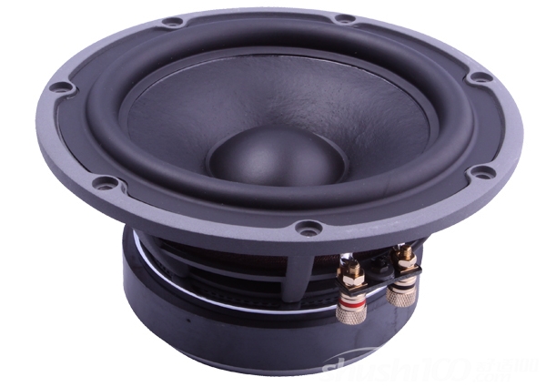
In today's consumer electronics market, miniature speakers are already used in a wide variety of devices, including gaming devices, smart home iot devices, and wearables. While private electronics that are turned up loud in public are often annoying, you will certainly prefer those that have a wider loudness range while ensuring fidelity at the time of purchase
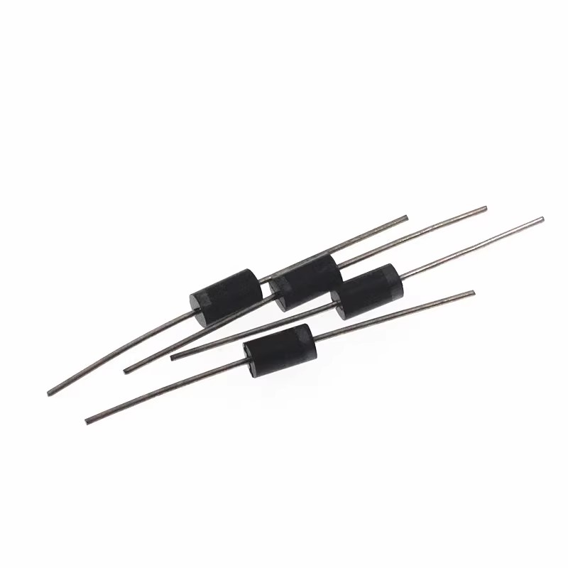
This paper studies ideal diodes with back-to-back MOSFETs as well as other more advanced devices. An ideal diode solution that integrates multiple functions to provide overall system protection is also presented. Diodes are very useful devices and are important for many applications. Standard silicon diodes have a voltage drop of 0.6V to 0.7V. The Schottky diode has a voltage drop of 0.3V. In general, the voltage drop is not a problem, but in high current applications, the individual voltage drops can produce significant power losses. Ideal diodes are ideal devices for such applications.

Technology companies and major semiconductor manufacturers are actively seeking ways to minimize their carbon footprint and thus achieve net zero greenhouse gas emissions. Under the 2015 Paris Agreement, the goal is to limit global warming to 1.5°C by 2050.
Voltage monitors improve the reliability of microcontroller-based systems by monitoring the power supply and putting the microcontroller into reset mode in the event of a power failure, preventing system errors and failures. However, power supply defects such as noise, voltage burrs, and transients can all cause false reset problems that can affect system behavior. This article describes how the voltage monitor can improve system performance and reliability by addressing factors that can trigger false reset.
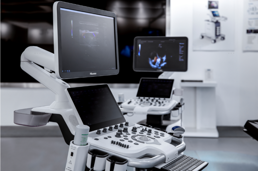
Ultrasound refers to sound waves with frequencies higher than 20,000 Hertz, which have specific applications in industrial and medical fields. With the progress of medical technology and the continuous update of equipment, ultrasound has become an indispensable application technology in the medical field.

Many systems require battery power. Batteries can be used to provide backup power in the event of a power outage, but are mostly used in mobile devices - as large as electric cars and as small as hearing AIDS. In all battery-powered systems, power efficiency is key. In the case of the same running time, the lower the power efficiency, the larger the battery will be, and the higher its cost.

How can e-mobility and sustainable energy ecosystems create and deliver greater value to electric vehicle (EV) owners? Analog Devices' electrification solutions product line, Analog Devices Recharge, offers a new definition. ADI Recharge improves electric vehicle operation and increases the lifetime value of the battery, ultimately helping to reduce the total cost of ownership of electric vehicles. ADI is working with Oems, Tier 1 suppliers, battery manufacturers, power companies and other stakeholders to build an unprecedented information ecosystem using EV battery data.
This paper will explore operational amplifiers suitable for electrochemical gas sensor applications such as ethanol and carbon monoxide (CO). The amplifier performance required for such applications will also be discussed to help ease portable devices accurately measure ethanol and CO with lower power consumption and better results.
Multiplex applications have some common requirements: there are many channels that need to be monitored. In general, an ADC monitors all channels sequentially; Channel voltages are usually independent of each other; There are strict limitations in terms of system size and power consumption. Because of these requirements, designers face some challenges.
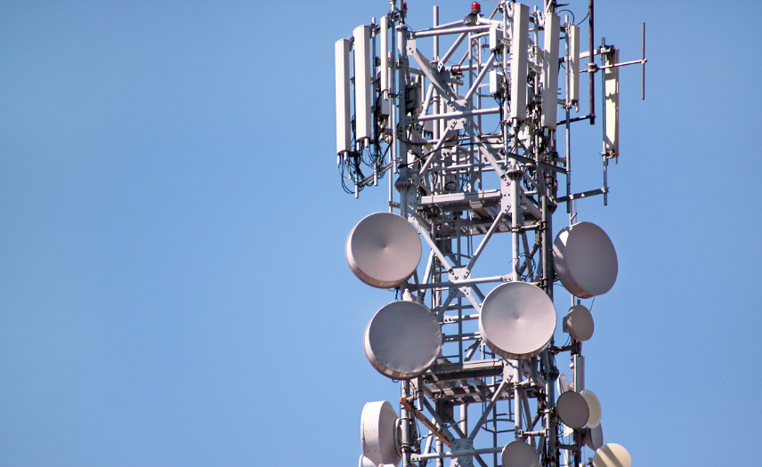
As new markets and applications continue to emerge, the demand for mobile data has skyrocketed. There is no solution other than deploying more cellular sites at greater density. These factors will directly affect the design of macro base station, small base station and femtobase station products. Now that radios support multi-band operation, power amplifier (PA) design engineers are trying to push the output power of PA to higher limits/levels.

As systems become more data-centric, monitors in industrial, iot, home medical wearables, fitness and health are experiencing explosive growth. These data-centric systems are increasingly demanding more features and lower power consumption. This trend is driven by intelligent systems that actively monitor a person or environment and make predictive responses, including alarms, actions, or recommended actions.
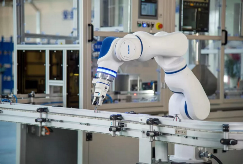
Giving the robot the ability to perceive and move the environment makes the robot safer and more mobile. If combined with Artificial Intelligence (AI) technology, it will make the robot smarter and more practical, making the future development of robots very imaginative space. This article will explore the development of robot perception and AI technology, as well as the related solutions introduced by many manufacturers.
There are thousands of different switching regulators on the market, and users choose the type they want based on different parameters, such as input voltage range, output voltage range, maximum output current, and many other parameters. In this article, ADI introduces current mode, an important feature commonly found in data books, and analyzes the advantages and disadvantages of this mode.

Analog Devices, the world's leading semiconductor company, has announced a €630 million investment in a new 45,000 sq ft advanced R&D and manufacturing facility at its European regional headquarters in Raheen Business Park, Limerick, Ireland.
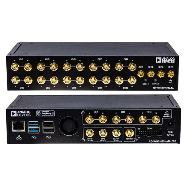
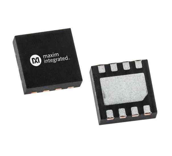
AD-SYNCHRONA14-EBZ is a standalone device that is ideal for evaluation and prototyping applications that require high precision frequency and phase control source clocks. Based on AD9545 and HMC7044, the device greatly simplifies clock allocation and multi-channel synchronization in complex systems
Under the booming development, as the application model project of industrial Internet deployment, predictive maintenance is expected to become one of the killer applications of IIoT (Industrial Internet of Things). In particular, the enabling of sensor technology and artificial intelligence algorithm greatly enhances its practicability and greatly improves its prediction accuracy. ADI Smart Motor Senor (SMS) is a typical predictive maintenance product design
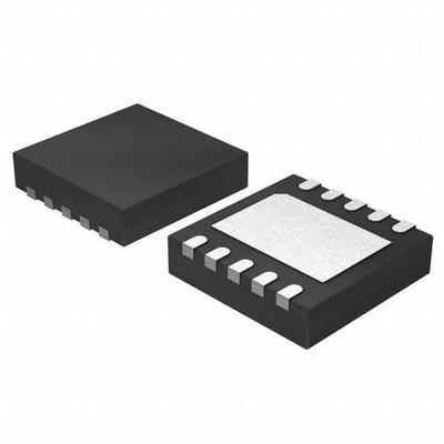
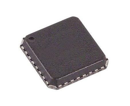
HMC900LP5E is a six-order, programmable bandwidth, fully calibrated, double low-pass filter. It has 0 or 10 dB input gain Settings, supports arbitrary bandwidth from 3.5 MHz to 50 MHz, and when calibrated, is accurate to +/-2.5% of the required bandwidth. It is packaged in a compact 5x5mm SMT QFN package that requires minimal external components, providing a low cost alternative to more complex switched discrete filter architectures.