The ISL6227 dual PWM controller provides efficient and precise voltage regulation with two synchronous step-down DC/DC converters. It is specifically designed to provide power conditioning for DDR memory, chipsets, graphics, and other system electronics in laptops.
The ISL6227's wide input voltage range capability allows voltage conversion directly from an AC/DC adapter or lithium-ion battery pack. Automatic mode conversion of constant frequency synchronous rectification under heavy loads and hysteretic (HYS) diode simulation under light loads ensure high efficiency under a wide range of conditions.
Universal application circuit
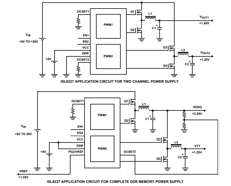
If constant frequency continuous on-off operation is required for all load levels, HYS mode of operation can be disabled separately on each PWM converter. Efficiency is further improved by using a lower MOSFET rDS(ON) as the current sensing element. Voltage feedforward ramp modulation, current mode control, and internal feedback compensation provide fast responses to input voltage and load transients. Input current ripple is minimized by a channel-to-channel PWM phase shift of 0°, 90°, or 180°(as determined by the input voltage and the state of the DDR pin). The ISL6227 can control two independent output voltages from 0.9V to 5.5V, or convert to a complete DDR storage power solution by activating DDR pins.
Pinouts

In DDR mode, the CH2 output voltage VTT tracks the CH1 output voltage VDDQ. The CH2 output can provide both source and sink current, which is the basic power feature of DDR memory. The reference voltage VREF required for DDR memory is also generated. In dual-power applications, the ISL6227 monitors the output voltage of the CH1 and CH2. After the soft-start sequence is complete, each channel asserts an independent PGOOD(power good) signal with the output voltage within the PGOOD window. In DDR mode, CH1 produces only PGOOD signals. Built-in overvoltage protection prevents output from exceeding 115% of the set value by keeping low MOSFeTs and high MosFeTs off.
Block Diagram

When the output voltage enters the adjustment state again, the PGOOD changes to HIGH and automatically resumes normal operation. Once the soft start sequence is complete, undervoltage protection locks the failure channel if the output drops below 75% of its set value. Voltage drop ON the rDS(ON) of the MOSFET under adjustable overcurrent protection (OCP). If more accurate current sensing is required, external current sensing resistors can be used.
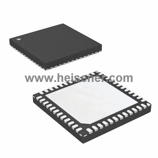
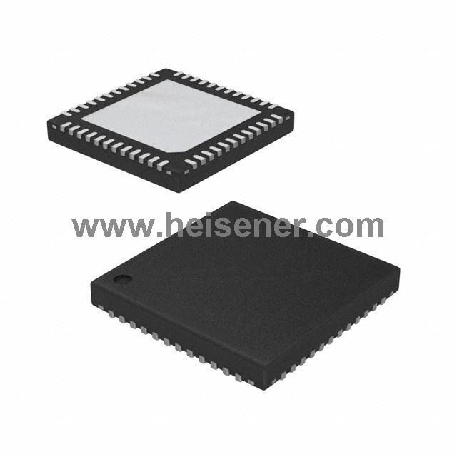
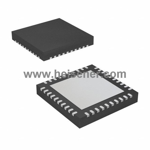
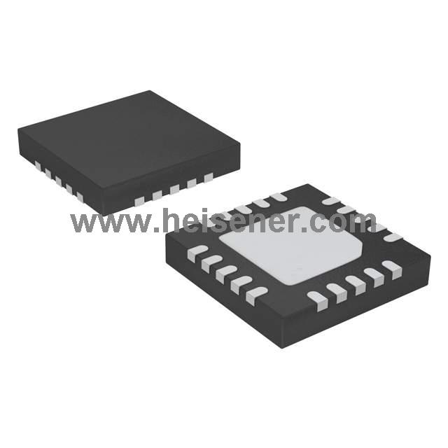
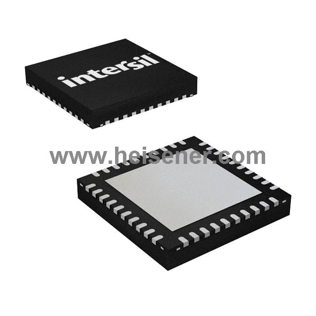
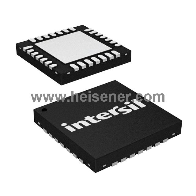
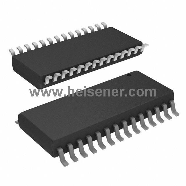
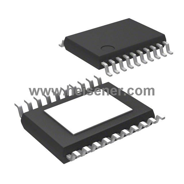
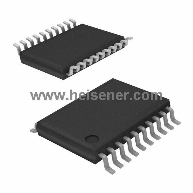
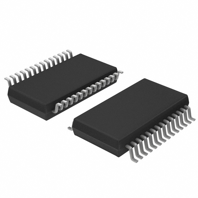
Package Outline Drawing