The AD9514 uses a multi-output clock distributed IC design that emphasizes low jitter and phase noise to maximize data converter performance. Other applications with phase noise and jitter requirements also benefit from this section. There are three separate clock outputs. Two of the outputs are lvvpecl, and the third output can be set to LVDS or CMOS level. The LVPECL output operates at 1.6 GHz, and the third output operates at 800 MHz in LVDS mode and 250 MHz in CMOS mode.
Schematic diagram

Each output has a programmable divider that can be set to divide by a selected set of integers between 1 and 32. The phase of one clock output with respect to another clock output can be set by a frequency division phase selection function as a coarse timing adjustment. LVDS/CMOS outputs a delay element with three optional full-range delay values (1.5ns, 5ns and 10ns), each with 16 steps of fine adjustment. The AD9514 requires no external controller to operate or set up.
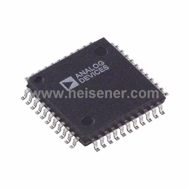
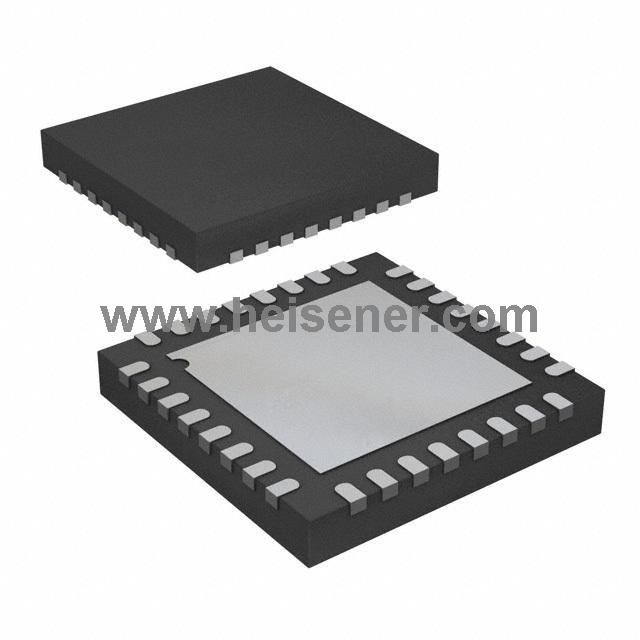
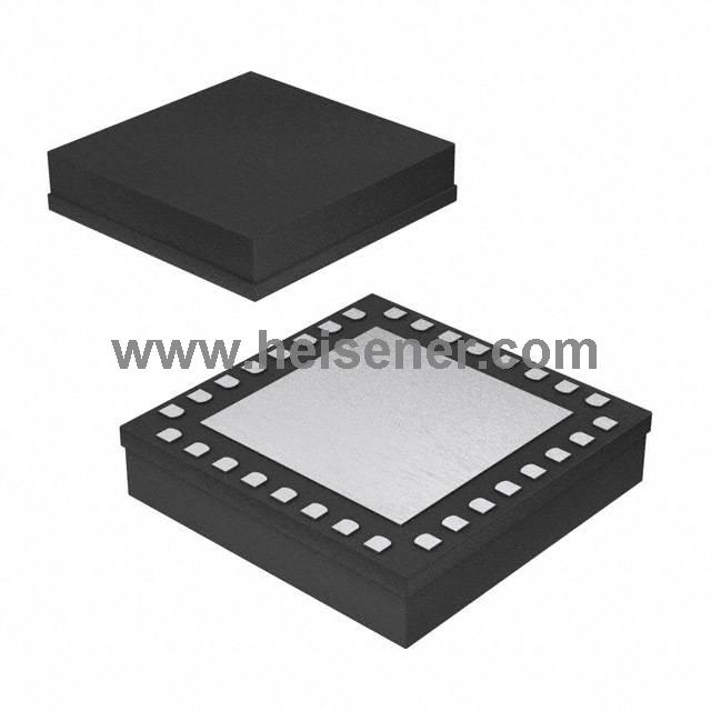
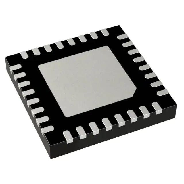
The device is programmed using 4-level logic with 11 pins (S0 to S10). Programming pins internally bias 1/3 vs. VREF pins provide level 1/3 vs. VS (3.3V) and GND (0 V) provides the other two logic levels. The AD9514 is ideal for data converter clock applications where maximum converter performance is achieved with subpicosecond jitter by encoding the signal. It uses 32 pin LFCSP and works with a single 3.3V power supply. The temperature ranges from −40 ° C to +85 ° C.
Features
● 1.6 GHz differential clock input
● 3 programmable dividers
● Divide-by in range from1 to 32
● Phase select for coarse delay adjust
● 2 independent 1.6 GHz LVPECL clock outputs
● Additive broadband output jitter 225 fs rms
● 1 independent 800 MHz/250 MHz LVDS/CMOS clock output
● Additive broadband output jitter 300 fs rms/290 fs rms
● Time delays up to 10 ns
● Device configured with 4-level logic pins
● Space-saving, 32-lead LFCSP