The FAN6555 switching regulator is designed to convert the voltage from 2.3v to 4v to the output voltage or stop voltage required for DDR SDRAM memory. It can achieve the production of a stabilized output voltage in two different modes. In default mode, the FAN6555 output voltage is 50% of the voltage applied to the vccq when the vref pin is on.
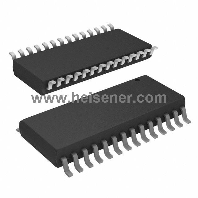
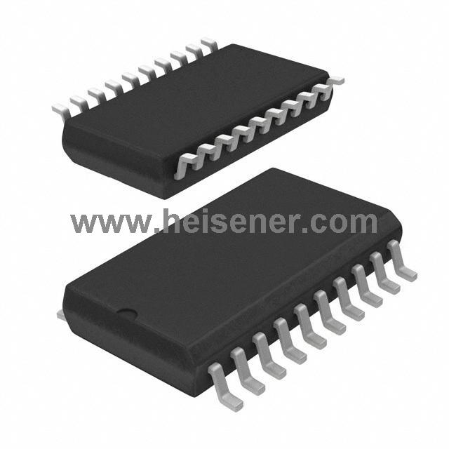
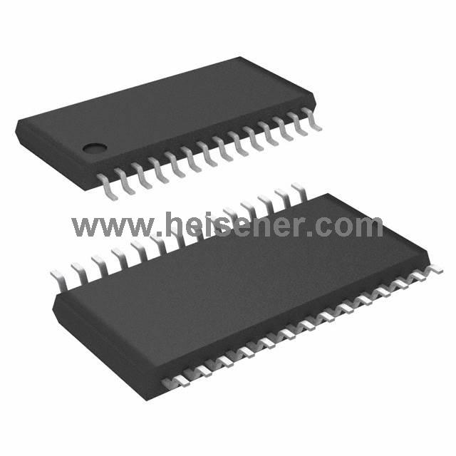
Pin Configuration

The FAN6555 can also generate a variety of user-defined voltages by applying voltage to the vrefin pin. In this case, the output voltage follows the input vrefin voltage. Switching regulators can source or sink up to 2a of current while regulating the output vtt voltage to 3% or less. Transient output currents of ±3a can also be adapted.
FAN6555 can also be used with series termination resistors to provide an excellent voltage source for active termination schemes for high-speed transmission lines, as seen in high-speed memory bus and distributed backplane designs.
Block Diagram
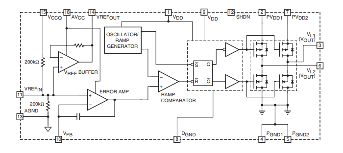
Function description
The FAN6555 integrates two power MosFeTs that can be used for source current and absorption 2A while maintaining strict voltage regulation. With external feedback, the output can be nicely tuned at 3% or less, depending on the external component selected. Separate voltage supply inputs have been added to suit the application with various power supply data and power bus.
Outputs
The output voltage pins (VL1, VL2) are connected to the data line, address line, or clock line via an external inductor. See the Application section for recommendations. The output voltage is determined by the VCCQ or VREFIN input.
Input voltage pins (VCCQ or VREFIN) determine the output voltage (VL1 or VL2). In default mode, the VREFIN pin is floating and the output voltage is 50% of the VCCQ input. VCCQ can be used as a reference voltage for the data.
Inputs
The output voltage can also be selected by applying a voltage to the VREFIN pin. In this case, the output voltage follows the input voltage of the VREFIN. In this case, a simple voltage divider can be used to produce a variety of output voltages between 0.7V and VDD-0.7V.
Input and output
The VREFIN input can be used to force the output voltage (input section above). The VREFOUT pin is an output pin, driven by a small output buffer, that provides the VREF signal to other devices in the system. The output buffer can drive multiple output loads. The output buffer can handle 3mA.
Other supply voltage
The supply voltage has several inputs :PVDD1, PVDD2, AVCC, and VDD. PVDD1 and PVDD2 supply the power for the power mosfet. The VDD provides voltage for the digital part and the AVCC provides voltage for the analog part.
Feedback input
The VFB pin is an input that can be used for closed-loop compensation. The input comes from the voltage output. See the Application section for recommendations.

Functional block diagram
Features
● Can source and sink up to 2A continous, 3A peak
● No heatsink required
● Integrated Power MOSFETs
● Generates termination voltages for DDR SDRAM
● VREF input available for external voltage divider
● Separate voltages for VCCQ and PVDD
● Buffered VREF output
● VOUT of ±3% or less at 2A
● Minimum external components
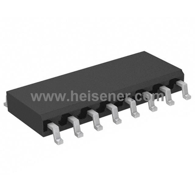
● 16-pin SOIC package
● -40°C to +85°C operating temperature range
● Shutdown for standby or suspend mode operation
● Thermal Shutdown ≈ 130ºC