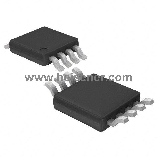
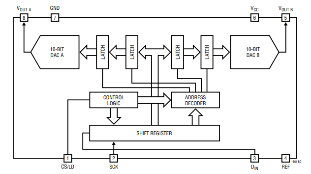
The LTC1661 integrates two precise, serial-addressable 10-bit digital-to-analog converters (Dacs) in a tiny MS8 package. Each buffer DAC draws only 60 μA of total supply current, but is capable of delivering over 5mA of DC output current and reliably driving capacitor loads up to 1000µF.
Sleep mode further reduces the total power current to a negligible 1μa. Linear Technology's proprietary inherently monotone voltage interpolation architecture provides excellent linearity while allowing for unusually small external form factors. The dual buffered input logic provides synchronous update functionality that can be used to write to either DAC without interrupting sleep mode.
Ultra-low power supply current, power-saving sleep mode and extremely compact size make the LTC1661 ideal for battery-powered applications, while its immediate availability, high performance and wide power range make it an excellent choice for general-purpose converters.
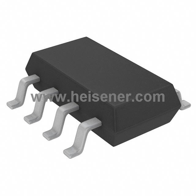
LTC1661 Pin arrangement

Pin function
CS/LD (Pin 1): Serial Interface Chip Select/Load Input. When CS/LD is low, SCK is enabled for shifting data on DIN into the register. When CS/LD is pulled high, SCK is disabled and the operation(s) specified in the control code, A3-A0, is (are) performed. CMOS and TTL compatible.
SCK (Pin 2): Serial Interface Clock Input. CMOS and TTL compatible.
DIN (Pin 3): Serial Interface Data Input. Input word data on the DIN pin is shifted into the 16-bit register on the rising edge of SCK. CMOS and TTL compatible.
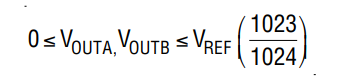
REF (Pin 4): Reference Voltage Input. 0V ≤ VREF ≤ VCC. VOUT A,
VOUT B (Pin 8, Pin 5): DAC Analog Voltage Outputs. The output range is
VCC (Pin 6): Supply Voltage Input. 2.7V ≤ VCC ≤ 5.5V.
GND (Pin 7): System Ground
LTC1661 Block Diagram
LTC1661 Timing Diagram

Features
● Tiny: Two 10-bit Dacs in an 8-pin MSOP -Half the board space of the SO-8
● Micropower :60µA/DAC Sleep Mode :1µA extends battery life
● Track voltage output drives 1000pF
● Wide power supply range of 2.7V to 5.5V
● Double buffering independently or simultaneously DAC update
● Reference range includes ratio metering supply 0V-to-Vcc output
● The reference input has a constant impedance Code (260kΩ Typ) - Eliminates the external buffer
● Three-wire serial interface with Schmidt trigger input
● Differential nonlinearity :≤±0.75LSB Max
Applications
● Mobile communication
● Digital control amplifier and attenuator
● Portable battery powered instrument
● Automatic calibration manufacturing
● Remote industrial device