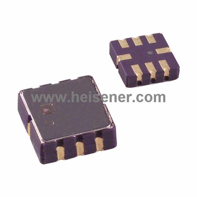
The LT1767 is a 1.25MHz monolithic step-down switch regulator. The regulator comes in an 8-pin leaded frame package and a low thermal resistance exposed liner package. Provides full cycle cycle term flow and thermal shutdown. High frequency operation allows for reduced input and output filtering elements and allows the use of chip inductance molds including A high efficiency 1.5A 0.22Ω switch, as well as all the control circuits required to complete the high frequency current mode switch regulator. Current mode control provides fast transient response and good loop stability.
Typical Application

The new design technique achieves high efficiency at high switching frequencies over a wide operating range. Low voltage internal regulators maintain consistent performance across a wide range of inputs from 24V systems to lithium-ion batteries. A working supply current of 1mA can improve efficiency, especially if the output current is low. The shutdown reduces the static current to 6µA. The maximum switching current remains constant at all duty ratios. Synchronization allows the external logic level signal to increase the internal oscillator from 1.5MHz to 2MHz.
Introduction to working principle
The LT1767 is a constant-frequency, current-mode step-down converter. This means that there is an internal clock and two feedback loops that control the duty cycle of the power switch. In addition to the normal error amplifier, there is a current sensing amplifier that monitors the switching current from cycle to cycle. A switching cycle is started by an oscillator pulse that sets the RS trigger to turn on the switch. When the switching current reaches the level set by the inverter input of the comparator, the trigger is reset and the switch is off. Output voltage control uses the output of the error amplifier to set the switch current trip point.
This technique means that the error amplifier commands the current to be passed to the output rather than the voltage. The voltage feed system will have a low phase shift up to the resonant frequency of the inductor and output capacitance. And then you have a 180 degree mutation. The current feed system will have a 90° phase shift at a much lower frequency, but there will be no additional 90° shift until well beyond the LC resonant frequency. This makes the frequency compensation feedback loop easier and also provides a faster transient response.
High switching efficiency is achieved by saturating the switch by using BOOST pins to supply a voltage higher than the input voltage to the switch driver. This boost voltage is generated by external capacitors and diodes. The comparator connected to the closing pin disables the internal regulator, reducing the supply current
Block Diagram