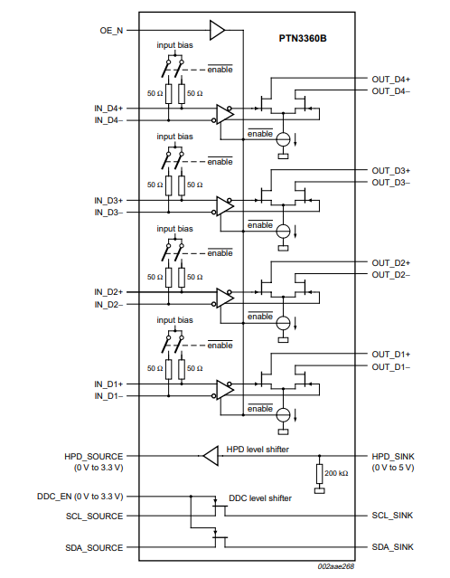
The PTN3360B is a high speed level converter that converts four-channel low-amplitude AC-coupled differential input signals into DVI v1.0 and HDMI v1.3a compatible leak-open current-directed differential output signals up to 2.5 Gbit/s per channel. Each of these channels provides a level-shift differential buffer to convert from a low-swing AC-coupled differential signal at the source to a tmds type DC-coupled differential current mode signal, terminating at 50 Ω to 3.3V at the receiver.
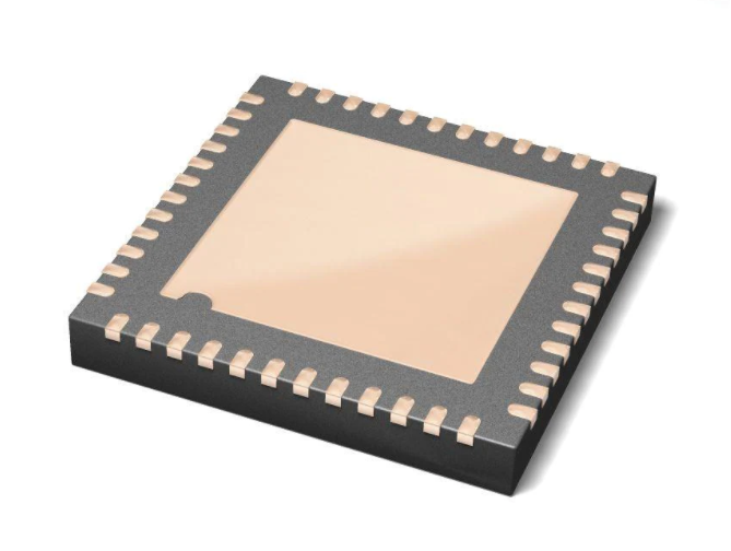
Pin arrangement

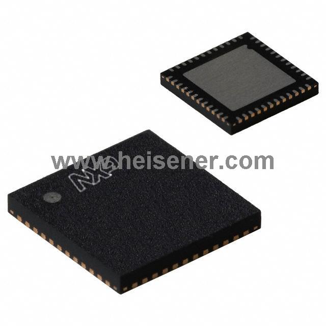
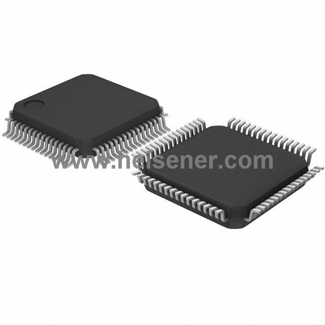
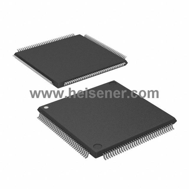
The PTN3360B is also a full-featured HDMI and DVI level converter. It is functionally comparable to the PTN3300A, but with higher speed performance and greater ESD robustness. PTN3360B is also equivalent to PTN3360A except that PTN3360B provides non-reverse level shift on the HPD channel. The PTN3360B is powered by a single 3.3V power supply with low power consumption (typical power is 120 mW) and is packaged with 48 terminals HVQFN48.
In addition, the PTN3360B provides a single-ended active buffer for converting the HPD signal from a 5v voltage at the receiver to a 3.3V voltage at the source, and a channel for level conversion in the DDC channel (consisting of clock and data lines) between the 3.3V source and 5v receiver ends. DDC channels are implemented using gate technology, providing level drift and clock and data line disabling (isolation between source and receiver).
The PTN3360B's low-swing AC coupled differential input signals typically come from a display source with multi-mode I/O that supports multiple display standards, such as DisplayPort, HDMI, and DVI. Although the input differential signals are configured to carry DVI or HDMI-encoded data, they do not meet the electrical requirements of the DVI v1.0 or HDMI v1.3a specifications. By using the PTN3360B, chipset vendors are able to implement this reconfigurable I/O on multi-mode display source devices, allowing support for multiple display standards while keeping the number of chipset I/O pins low. See the picture below
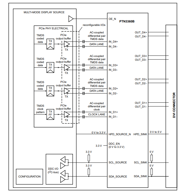
The PTN3360B main high-speed differential channel has a low-swing self-biased differential input conforming to the electrical specifications of DisplayPort standard v1.1 and/or PCI Express standard v1.1, and leak-current flow conforming to the electrical specifications of DVI v1.0 and HDMI v1.3a to the differential output. i2c bus channel level conversion DDC signals are between 3.3V (source) and 5.0V (receiver).
Functional diagram
Features
High-speed TMDS level shifting
● Converts four lanes of low-swing AC-coupled differential input signals to DVI v1.0 and
● HDMI v1.3a compliant open-drain current-steering differential output signals
● TMDS level shifting operation up to 2.5 Gbit/s per lane (250 MHz character clock)
● Integrated 50 Ω termination resistors for self-biasing differential inputs
● Back-current safe outputs to disallow current when device power is off and monitor is on
● Disable feature to turn off TMDS inputs and outputs and to enter low-power state
DDC level shifting
● Integrated DDC level shifting (3.3V source to 5 V sink side)
● 0 Hz to 400 kHz I2C-bus clock frequency
● Back-power safe sink-side terminals to disallow backdrive current when power is off or.
● Back-power safe sink-side terminals to disallow backdrive current when power is off or when DDC is not enabled
2.3 HPD level shifting
● HPD non-inverting level shift from 5 V on the sink side to 3.3V on the source side, or from 0 V on the sink side to 0 V on the source side
● Integrated 200 kΩ pull-down resistor on HPD sink input guarantees' input LOW 'whenno display is plugged in
● Back-power safe design on HPD_SINK to disallow backdrive current when power is off 2.4
General
● Power supply 3.3V ± 10%
● ESD resilience to 8 kV HBM and 500 V CDM
● Power-saving modes (using output enable)
● Back-current-safe design on all sink-side main link, DDC and HPD terminals
● Transparent operation: no re-timing or software configuration required