The four output CMOS buffers/drivers of the MIC4467/8/9 series are extensions of earlier single and dual output drivers, which are closely related in function. As the number of package pins allows, each drive is equipped with dual input logic gates for added flexibility. Placing four high-power drivers in a single package also improves system reliability and reduces total system cost.
In some applications, one of the drivers can replace not only two single-input driver packages, but also some of the associated logic. While primarily used to drive power mosFeTs and similar high-capacitance loads, these drivers are equally suitable for driving any other load (capacitive, resistive, or inductive) that requires high-efficiency, low-impedance drivers capable of achieving peak current, rail-to-rail voltage fluctuations, and fast switching times.
For example, heavy-duty clock lines, coaxial cables, and piezoelectric sensors can all be easily driven with the MIC446x series driver. The only limitation to loading is that the total power consumption of the IC must remain within the power consumption limit of the package. The MIC446x family of drivers is built using the BCD process.
They do not latch in any condition within the power and rated voltage range. They are not damaged when noise peaks of up to 5V (of any polarity) occur on the ground wire. They can accept up to half an amp of induced flyback current (of any polarity) to their output without damage or logic confusion.
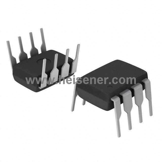
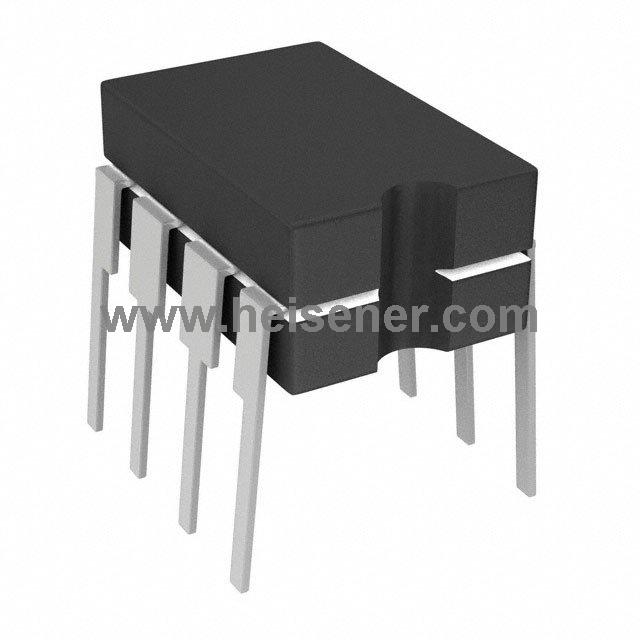
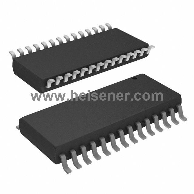
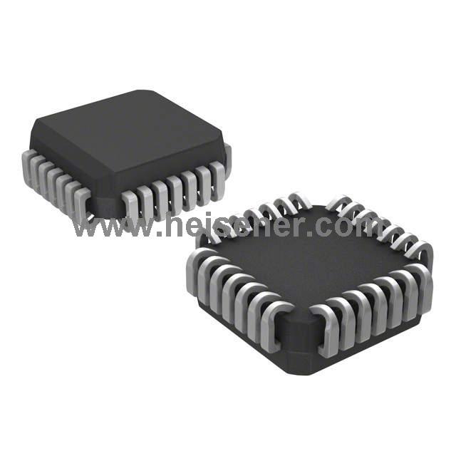
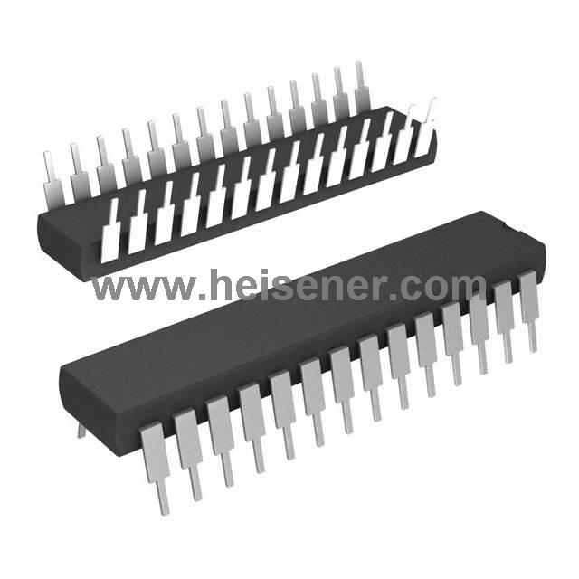
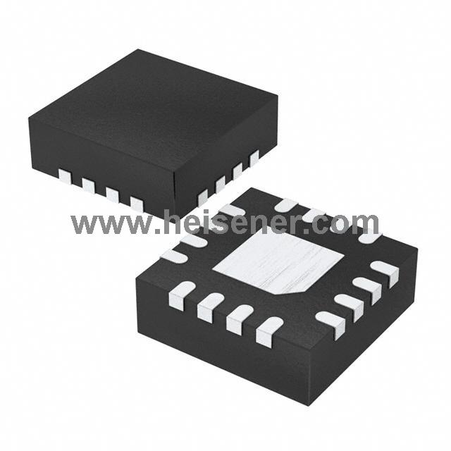
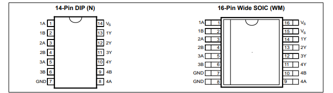
Pin arrangement
Logic Diagrams

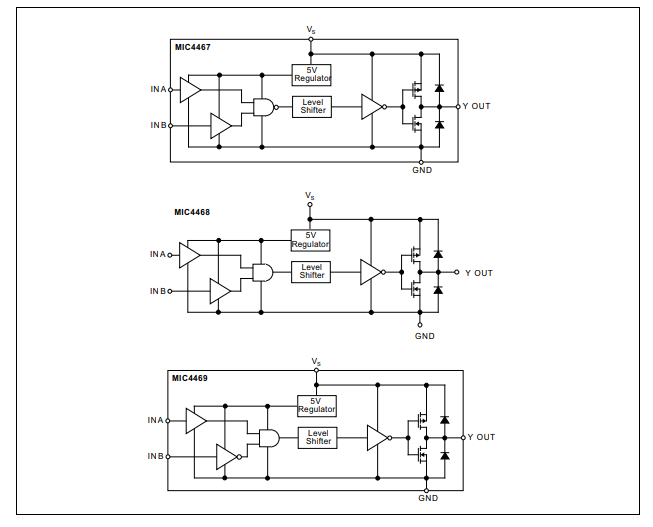
Block Diagrams
Features
• Reliable, Low-Power Bipolar/CMOS/DMOS Construction
• Latch-Up Protected to > • latch-up protected to > 500 mA Reverse Current
• Logic Input withstands Swing to -- 5V
• High 3A Peak Output Current
• Wide 4.5V to 18V Operating Range
• Symmetrical Rise and Fall Times
• Short < 40 ns Typical Delay Time
• TTL Logic Input Independent of Supply Voltage
• Low Equivalent of 6 pF Input Capacitance
• Low 5Ω Typical Output Impedance
• Output Voltage Swings within 25 mV of Ground or ground VS
Applications
• General-Purpose CMOS Logic Buffer
• Driving All 4 MOSFETs in an H-Bridge
• Direct Small Motor Driver
• Relay or Peripheral Drivers
• Dual Differential Output Power Drivers
• CCD Driver
• Pin Switching Network Driver