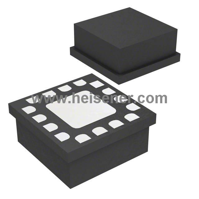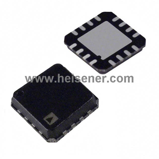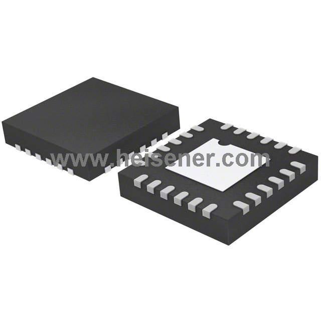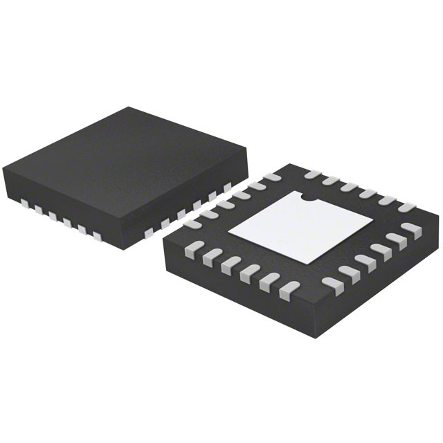
The ADCLK946 is an ultra-fast clock fan-out buffer manufactured from Analog Devices' proprietary XFCB3 silicon-germanium (SiGe) bipolar process and operating in standard industrial temperature ranges from −40°C to +85°C using a 24-pin LFCSP.
The ADCLK946 features six fully swing emitter coupled logic (ECL) output drivers. For LVPECL(positive ECL) operation, bias the VCC to the positive power supply and the VEE to the ground. For ECL operation, bias VCC to ground and VEE to negative power. The ECL output stage is designed to directly drive 800 mV to 50 Ω ends on each side to VCC−2 V, with a total differential output swing of 1.6 V.
Functional block diagram

The device is designed for high-speed applications requiring low jitter. The device has a differential input and is equipped with a center tap, differential, 100 Ω on-chip terminal resistor. Inputs accept DC coupled LVPECL, CML, 3.3V CMOS(single-ended) and AC coupled 1.8V CMOS, LVDS, and LVPECL inputs. VREF pins can be used to bias AC coupled inputs.
Function description
Clock input
The ADCLK946 accepts differential clock inputs and distributes them to all six LVPECL outputs. The maximum specified frequency is the point at which the output voltage swings to 50% of the standard LVPECL swing

The device has a differential input and is equipped with a center tap, differential, 100 Ω on-chip terminal resistor. Inputs accept DC coupled LVPECL, CML, 3.3V CMOS(single-ended) and AC coupled 1.8V CMOS, LVDS, and LVPECL inputs. VREF pins can be used to bias AC coupled inputs
If the input pendulum rate is lower than 1v /ns, the output jitter performance will be reduced. The ADCLK946 is specifically designed to minimize increased random jitter over a wide range of input conversion rates. Whenever possible, clamp large input signals with fast Schottky diodes because attenuators slow down the conversion rate. Input signals larger than a few centimeters should use low-loss media or cable with good high-frequency characteristics

Features
● 4.8 GHz operating frequency
● 75 fs rms broadband random jitter
● On-chip input terminations
● 3.3V power supply
Application
● Low jitter clock distribution
● Clock and data signal restoration
● Level translation
● Wireless communications
● Wired communications
● Medical and industrial imaging
● ATE and high performance instrumentation