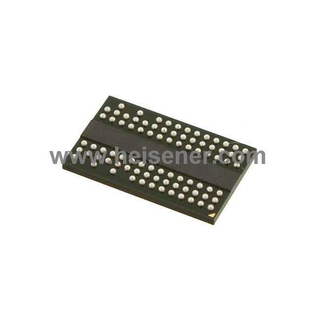
W9751G6KB-25 Introduction
The W9751G6KB-25 is a 512Mbit DDR2 SDRAM chip organized into 8,388,608 words across 4 banks, each 16 bits wide. It supports high-speed data transfer rates of up to 1066Mb/sec per pin (DDR2-1066), making it suitable for a variety of general applications. This memory chip is available in several speed grades, including -18, -18L, -25, -25L, -251, and -3. The -18 and -18L grades meet the DDR2-1066 specification with timings of 7-7-7 and are designed to operate within a temperature range of -40°C to 95°C.
The -25, -25L, and -251 grades comply with the DDR2-800 specification with timings of 5-5-5 or 6-6-6, while the -3 grade adheres to the DDR2-667 (5-5-5) specification. The W9751G6KB-25 features synchronized control and address inputs, which latch at the crossover of externally supplied differential clocks. Additionally, all I/O operations are synchronized using either a single-ended DQS signal or a differential DQS-DQS pair, enhancing its performance in source synchronous applications.
W9751G6KB-25 Pin Configuration

W9751G6KB-25 Symbol

W9751G6KB-25 Footprint

W9751G6KB-25 3D Model

W9751G6KB-25 Block Diagram

W9751G6KB-25 Specification
| Feature | Specification |
| Memory Density | 512 Mbits |
| Memory Organization | 32M x 16 |
| Memory Interface | Parallel |
| Clock Frequency | 400 MHz |
| Write Cycle Time - Word, Page | 15ns |
| Access Time | 57.5 ns |
| Voltage - Supply | 1.7V ~ 1.9V |
| Operating Temperature | 0°C ~ 85°C (TC) |
| Package | 84-WBGA |
W9751G6KB-25 Features
- Power Supply: VDD,VDDQ=1.8V±0.1V
- Double Data Rate architecture: two data transfers per clock cycle
- CAS Latency: 3, 4, 5, 6 and 7
- Burst Length:4and 8
- Bi-directional, differential data strobes are transmitted / received with data
- Edge-aligned with Read data and center-aligned with Write data
- DLL aligns DQ and DQS transitions with clock
- Differential clock inputs.
- Data masks(DM) for write data
- Commands entered on each positive CLK edge, data and data mask are referenced to both edges of DQS
- Posted CAS programmable additive latency supported to make command and data bus efficiency
- Read Latency = Additive Latency plus CAS Latency(RL=AL+CL)
- Off-Chip-Driver impedance adjustment(OCD) and On-Die-Termination (ODT) for better signal quality
- Auto-precharge operation for read and write bursts
- Auto Refresh and Self Refresh modes
- Precharged Power Down and Active Power Down
- Write Data Mask
- Write Latency=Read Latency-1(WL=RL-1)
- Interface: SSTL_18
- Packaged in WBGA 84 Ball (8X12.5 mm2), using Lead free materials with RoHS compliant
W9751G6KB-25 Applications
Consumer Electronics
Computers and Laptops
Networking Equipment
Automotive Applications
Industrial Applications
Telecommunications
W9751G6KB-25 Package
The W9751G6KB-25 is packaged in an 84-WBGA (Wire Bond Ball Grid Array) configuration, which offers a compact and efficient layout for modern electronic applications. This package features a 14mm x 14mm footprint with a ball pitch of 1.0mm, making it suitable for high-density designs. The 84-ball configuration allows for enhanced thermal and electrical performance, ensuring reliable connections in demanding environments.
The WBGA package design also facilitates improved heat dissipation, which is crucial for maintaining optimal operating temperatures during high-speed operations.

How to Use W9751G6KB-25?
When using the W9751G6KB-25 DDR2 SDRAM, the first step is to prepare the PCB. Place the W9751G6KB-25 precisely on the board according to the pin configuration of the 84-WBGA package, ensuring that the solder balls align with the pads. Use an appropriate soldering process, such as reflow soldering, to secure the chip.
After soldering, connect the VDD and VSS pins to the appropriate power supply. Next, configure the control pins (such as CS, RAS, CAS, and WE) and ensure that the address lines match the signals from the external microcontroller or processor. Additionally, provide external differential clock signals (CLK and CLK_B). All I/O pins should be paired with the DQS (Data Strobe) signal for proper synchronization.
Once these connections are complete, perform a power-on test to check if the W9751G6KB-25 is functioning correctly. If everything is in order, use appropriate testing software to validate read and write operations.
FAQs
What is the maximum data transfer rate for the W9751G6KB-25?
The device achieves data transfer rates of up to 1066 Mb/sec per pin (DDR2-1066) for general applications.
How is the W9751G6KB-25 synchronized with the control signals?
All control and address inputs are synchronized with a pair of externally supplied differential clocks, with inputs latched at the cross point of these clocks.
How do I connect the W9751G6KB-25 to my circuit?
To connect the W9751G6KB-25, ensure proper alignment on the PCB, connect VDD and VSS to the power supply, configure control pins, and provide differential clock signals along with DQS for I/O synchronization.